RTL INTEGRATION
About Course
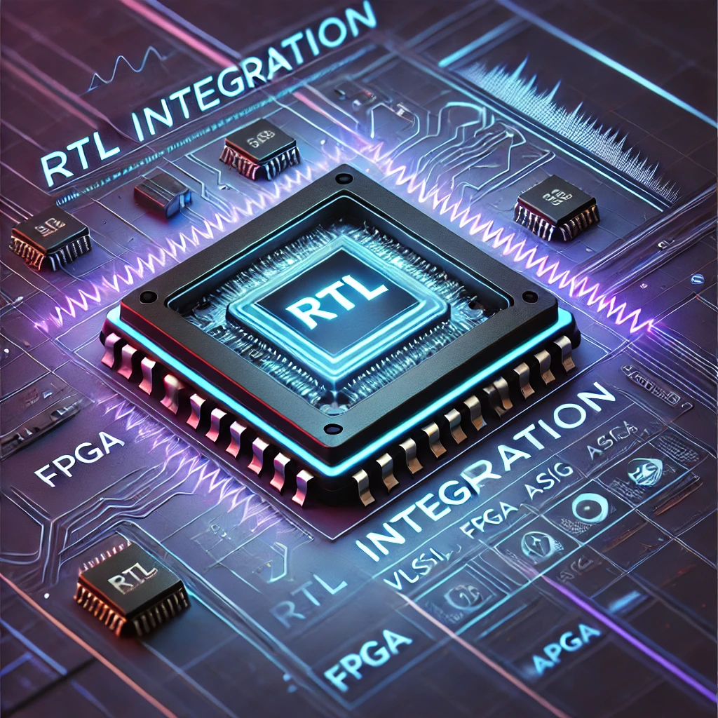
RTL Integration is one of the most critical and industry-relevant roles in the front-end VLSI design flow. Modern SoCs are rarely built from a single RTL block; instead, they consist of numerous IPs, subsystems, interfaces, clock domains, power domains, and design constraints that must be integrated correctly to create a functional and implementation-ready chip.
This course is designed to provide a comprehensive understanding of the RTL Integration process used in professional ASIC and FPGA development environments. Rather than focusing solely on RTL coding, the course explores how individual design blocks are integrated, analyzed, constrained, validated, and prepared for successful implementation.
Participants will learn the practical aspects of manual RTL integration, glue logic development, linting, clock domain crossing (CDC) analysis, power intent specification using UPF, timing constraint development, synthesis, logical equivalence checking (LEC), and static timing analysis (STA). These activities form the foundation of a successful RTL Integration workflow and are routinely performed in modern semiconductor projects.
By the end of the course, participants will possess a strong understanding of industry-standard RTL Integration methodologies and will be better prepared for RTL Design, RTL Integration, FPGA Design, and Front-End VLSI engineering roles.
Course Content
Introduction to RTL Design & Integration
-
Overview of RTL Design and Integration
-
ASIC & FPGA Design Flow
-
Role of an RTL Integrator in the VLSI Industry
RTL Development and Manual Integration
Linting and CDC (Clock Domain Crossing) Analysis
Power Intent and Low-Power Design (UPF)
XDC and Timing Constraints
Synthesis and Logical Equivalence Checking (LEC)
Static Timing Analysis (STA)
Student Ratings & Reviews

No Review Yet